NanoImpulse
LiveA local TEM/SEM measurement desk for real-space images, diffraction patterns, and core-loss EELS spectra.
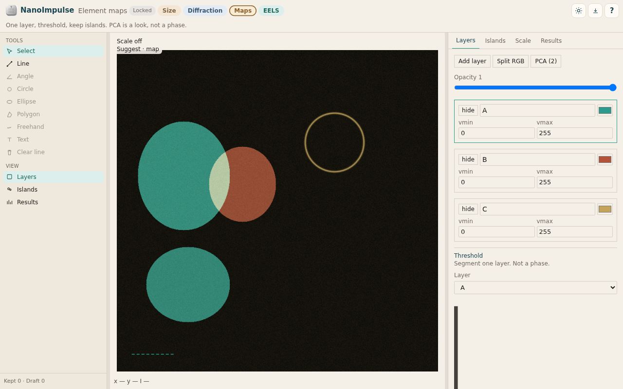
NanoImpulse is a local TEM, STM, SEM, EDS/Raman maps and general micrographs analysis desk for real-space images, with additional powerful tools for diffraction patterns, and core-loss EELS spectra.
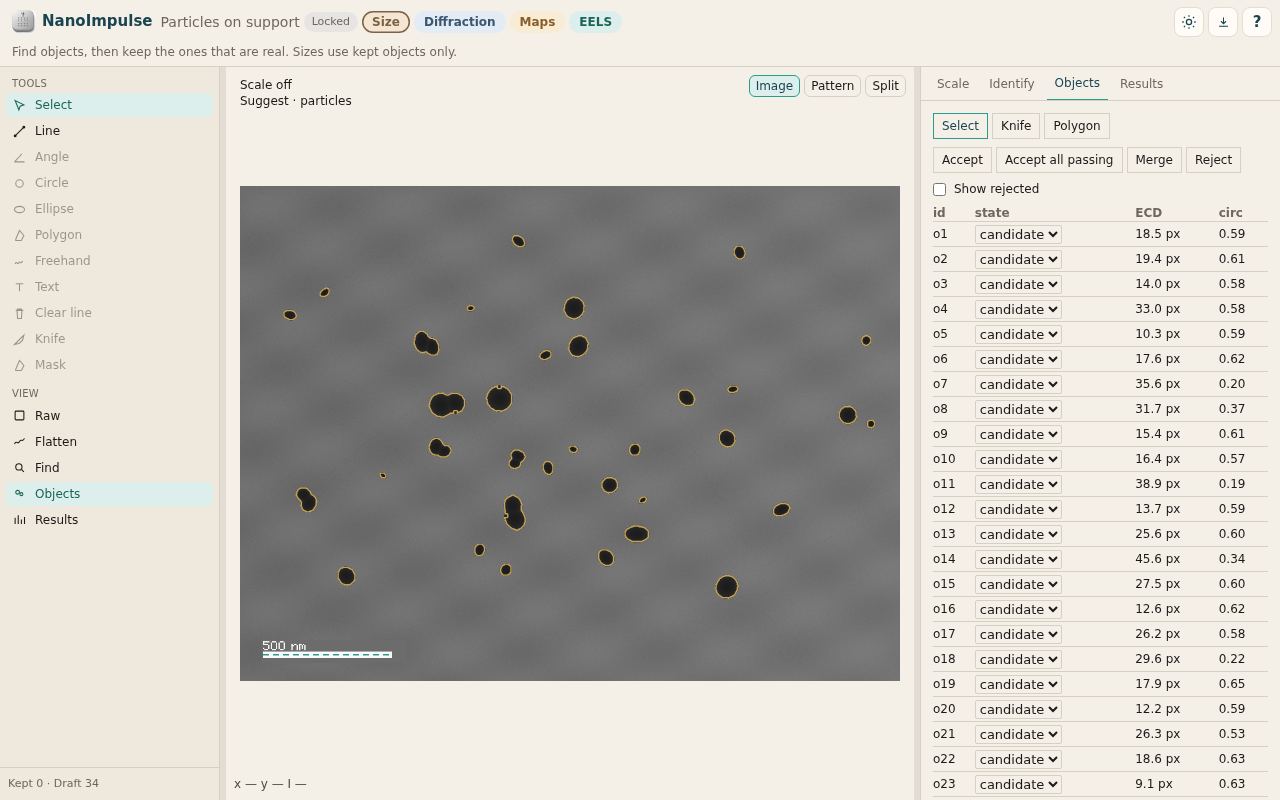
Particle and grain finding is only a candidate list: sizes, aspect ratios, and nearest-neighbour distances are computed from the objects you keep, not from every segmented region. A line across lattice fringes gives d = L/N only after you enter the integer fringe count N. That length is not a grain size.
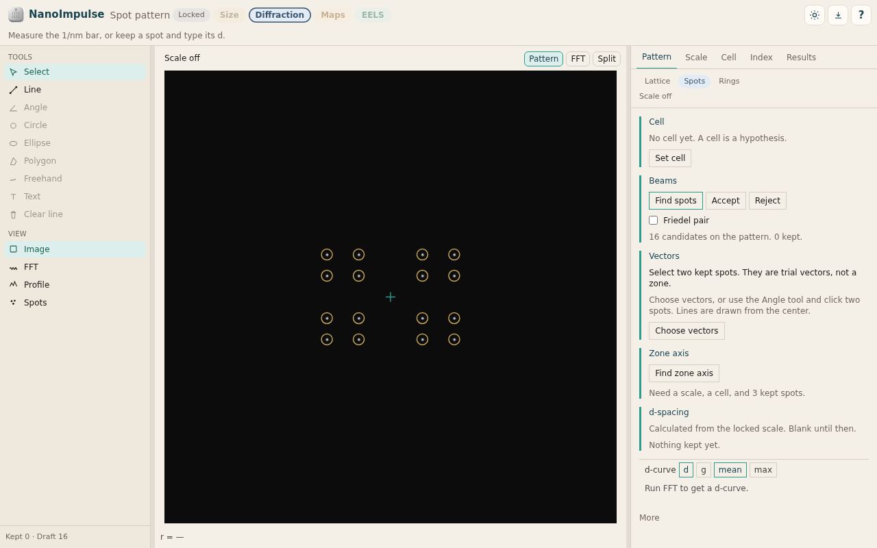
A SAED pattern is measured in the pattern, not by taking its FFT. Spots are picked from local intensity maxima, with an optional Friedel pair snapped to a real peak. Rings come from the radial profile, with a dark beam-stop excluded from the average. d-spacings stay blank until a reciprocal scale is set, either from a known d or from a real-space scale that supplies Δk (1/nm per pixel) and the camera constant Lλ in px·nm. Two chosen g vectors are used to index a zone against a cell loaded from a CIF. That cell is a trial lattice. It is not a phase identification, and no kV or camera constant is filled in if you did not enter it.
For core-loss EELS the spectrum is a power-law fit on the pre-edge window, subtracted under the signal window you set. A structured residual is reported as a bad background, not as an element. No k-factor and no edge assignment are inferred from the energy window.